- home
- 제품소개
- 장비사업
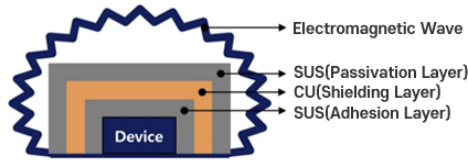
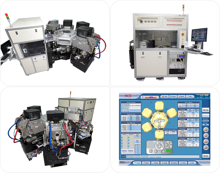
EMI Shield용(전자파 차폐) Sputtering System
반도체 소자 표면에 보호막을 증착하여 전자파를 차폐 시키는 기술을 적용한 시스템
Application : Semiconductor PKG, SAW Filter
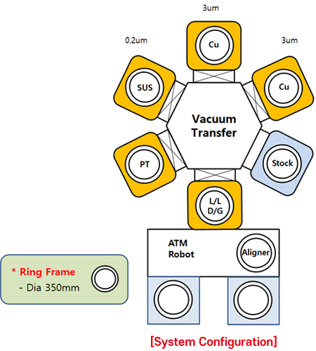
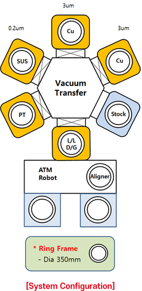
Cluster type
EFEM / Loadlock & Degassing / PT / Transfer / PM(SUS, Cu) / Stock
고품질 / 고균일 박막 형성
우수한 Step coverage 및 소자 보호를 위한 100℃이하 공정 구현
Target Erosion대비 증착 효율이 우수한 Round type cathode
낮은 COO(Cost of Operation)
높은 가동률, Small foot-print
| Items | Specifications | |
|---|---|---|
| System | System Control | Full Automation |
| Configuration | Cluster | |
| Thin Film | Total Thickness | SUS 0.2/ Cu 3.0/ SUS 0.2㎛ |
| Configuration | Source Type | Magnetron Cathode |
| Lamp Type Heater for Degassing | Max 150℃ on Substrate | |
| Substrate rotation sputtering | Rotation | |
| Magnet rotation sputtering | Rotation | |
| Plasma Treatment | ICP+RF Bias type | |
| Performance | Step Coverage | 〉 40% |
| Thickness Uniformity | 〈 3% (Top Layer) | |
| PKG Temperature Control | 〈 100℃ | |
| Contact Resistance | 〈 0.2Ω | |
| Peel off(Adhesion) | 5B(0%) | |
| SE(Shielding effectiveness) | 〉 75dB | |
| Plasma Contact angle | 5Degree | |
| CAPA | Tact Time (1Frame depo. time) | 〈 5mins |