- home
- Product
- Equipment business
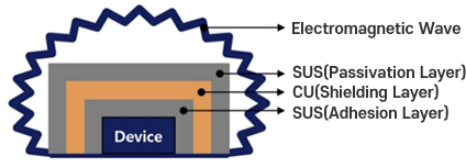
Sputtering System for EMI(Electro Magnetic Interference) Shield
A system applied with a technology to shield electromagnetic waves by depositing a protective film on the surface of a semiconductor device.
Application : Semiconductor PKG, SAW Filter
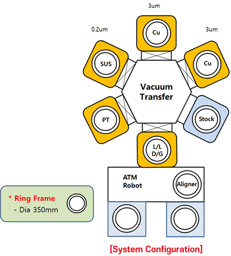
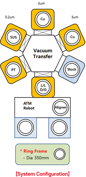
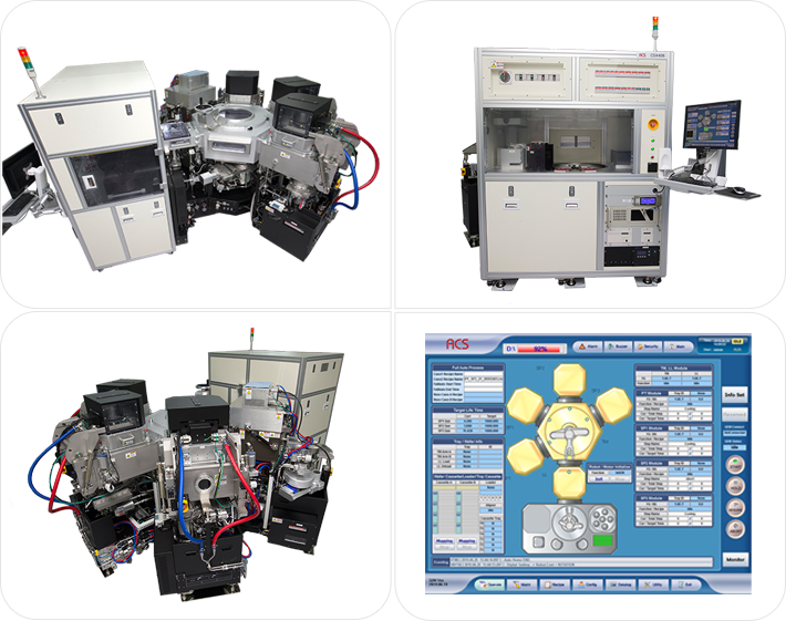
Cluster type
EFEM / Loadlock & Degassing / PT / Transfer / PM(SUS, Cu) / Stock
Formation of high quality / high uniformity thin film
Excellent step coverage / realization of process below 100℃ for device protection
Round type cathode with superior deposition efficiency compared to target erosion
Low COO(Cost of Operation)
High utilization, Small foot-print
| Items | Specifications | |
|---|---|---|
| System | System Control | Full Automation |
| Configuration | Cluster | |
| Thin Film | Total Thickness | SUS 0.2/ Cu 3.0/ SUS 0.2㎛ |
| Configuration | Source Type | Magnetron Cathode |
| Lamp Type Heater for Degassing | Max 150℃ on Substrate | |
| Substrate rotation sputtering | Rotation | |
| Magnet rotation sputtering | Rotation | |
| Plasma Treatment | ICP+RF Bias type | |
| Performance | Step Coverage | 〉 40% |
| Thickness Uniformity | 〈 3% (Top Layer) | |
| PKG Temperature Control | 〈 100℃ | |
| Contact Resistance | 〈 0.2Ω | |
| Peel off(Adhesion) | 5B(0%) | |
| SE(Shielding effectiveness) | 〉 75dB | |
| Plasma Contact angle | 5Degree | |
| CAPA | Tact Time (1Frame depo. time) | 〈 5mins |