- home
- 产品介绍
- 设备事业
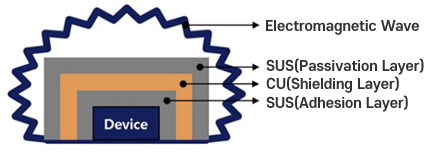
EMI Shield用(电磁波遮蔽) Sputtering System
为保护半导体器件,在表面镀保护膜来遮蔽电磁波的设备
Application : Semiconductor PKG, SAW Filter
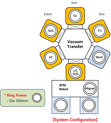
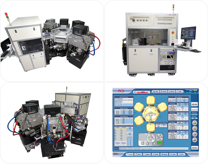
Cluster type
EFEM / Loadlock & Degassing / PT / Transfer / PM(SUS, Cu) / Stock
形成高品质 / 高均匀薄膜
优秀的 Step coverage 及实现100℃以下工艺技术
比Target Erosion 镀膜效率高的 Round type cathode
低的 COO(Cost of Operation)
高稼动率, Small foot-print
| Items | Specifications | |
|---|---|---|
| System | System Control | Full Automation |
| Configuration | Cluster | |
| Thin Film | Total Thickness | SUS 0.2/ Cu 3.0/ SUS 0.2㎛ |
| Configuration | Source Type | Magnetron Cathode |
| Lamp Type Heater for Degassing | Max 150℃ on Substrate | |
| Substrate rotation sputtering | Rotation | |
| Magnet rotation sputtering | Rotation | |
| Plasma Treatment | ICP+RF Bias type | |
| Performance | Step Coverage | 〉 40% |
| Thickness Uniformity | 〈 3% (Top Layer) | |
| PKG Temperature Control | 〈 100℃ | |
| Contact Resistance | 〈 0.2Ω | |
| Peel off(Adhesion) | 5B(0%) | |
| SE(Shielding effectiveness) | 〉 75dB | |
| Plasma Contact angle | 5Degree | |
| CAPA | Tact Time (1Frame depo. time) | 〈 5mins |